Knoppson Home-Brew CPU on a CPLD
This is the current schematic of my CPU. I use a CPLD manufatured
by Xilinx. This CPLD (XCR3512XL-7PQ208C) enables me to fit
a whole CPU architecture into a single chip. My CPU is however of a very
simple RISC design. It is even not able to do multiplications or divisions
but that will be solved with software because all you need is to be able to
add and shift. Right now the CPU shifting feature is however a bit limited.
It can only shift in zeroes and that will probably not do.
It should be noted that all programming of the CPLD has been done by gates.
This is possible due to Xilinx fanatastic tool called ECS. It is an integrated
part of the standard devoloping tool called ISE. While I suck at ordinary
programming this has helped me enormously and also kept my pride in saying
that this CPU has been designed using discrete gates only. There is one small
exception though, the SR-F/F's weren't able to be cadded this way due to some
over-intelligence in the optimizer. I therefore had to use a predefined JK-F/F
for all the counters and registers. Everything else has been designed by simple
gates.
This is the current layout of the CPU. I am wire-wrapping this because PCB
manufaturing is expensive and also the CAD program at work is hard for a novice
like me to understand. The Test Board is optionally removable if this project
ever will work. In that case I will build a keyboard as well as a monitor interface
instead of the Test Board.
This is the way my CPU-project looks right now. All the instruction register (IR)
signals have been wire-wrapped as well as unused CMOS input groundings and Chip Selects
Next step is to wire-wrap the Clock Module which will be of very primitive design.
It will only have three modes of operation. Single step (DC), Freerunning (0,5Hz initially),
and Freerunning with halt (holding switch upwards).
The goal of this project is not to build a fast CPU or even a fast computer, the goal is
to build a primitive and perhaps even useful CPU that actually works. I have therefore
concentrated on low clock speeds. However, The CPLD itself is good for at least 150MHz
and this is nice if it wasn't for my old EPROM's I am using to realize all the instructions
which limits theoretical maximum speed to some 4MHz.
This is the top view of my project right now. The huge area to the right will fit
the Schmart Board with the 208-pin CPLD. The Test Board on the left mainly consists
of two hexadecimal switches and dito registers which will enable me to test all CPU
instructions.

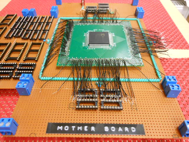
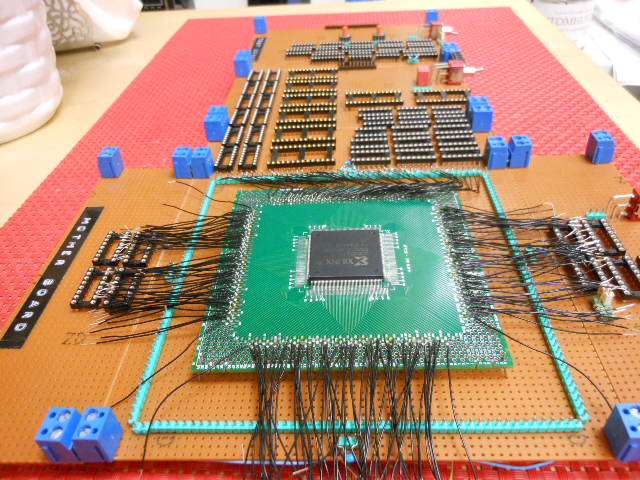
This picture shows all the 208 tiny wire-wrap wires assembled to the Schmart Board.

Here I have soldered one side of the huge CPLD.

This view is somewhat nicer even though my delicate work do not show.

Here is a fun picture of some of my IC modules. I searched and found tiny
LEDs which I handsoldered to these extremely expensive adaptors (about $4 each).
I colorcoded them in red and green to be able to more easily read the HEX code.

This picture shows the wire-wrapping at the finished state.

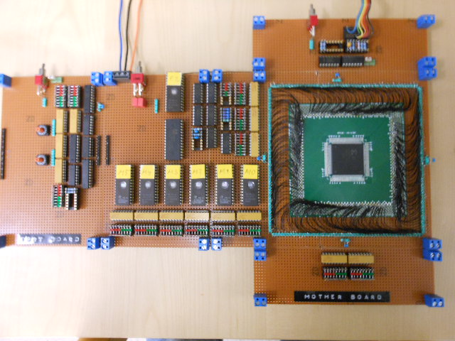
This is the top view of my CPU with all the ICs mounted. Down to the left
you can see the LEDs for all the 48 control signals generated by all the six
PROMs shown adjascent. Up to the left you have two LED-arrays (1 Byte).
The furthest to the left indicates whatever value I tune the tiny BCD-switches to.
When I am satisfied, I hit the right above switch and latch the set value
into the system. Furthest down to the left is the output-LED array which
is the only mean of communication I have with the CPU. Except for a huge
number of debug LEDs that is (over a hundred).
The middle switch is the POR-switch. I have an external supply that supplies
5V and 3,3V. When this switch goes on power is supplied and a special POR-
signal is generated. It is a glitch of approximatelly only 1us which sets
all registers and counters inside the CPLD to the correct start value.
This actually works.
The rightmost switch is the manual clock switch. Depending on a jumper you
can set if you want a DC-clock or an astable clock which you even can halt
as I have said above.
I have videos to prove that some small part of the CPU actually works.
Mainly this means that the internal RST-instruction actually works.
And it does actually do a true fetch/execute. At least to some primitive extent.
Due to Murphy I happened to microprogram that very first instruction wrongly
(out of 36, you do the math...).
Some videos:
This is a video of some very small success in the design of my CPU. Watch the three
green LEDs down to the right. They reflect each of the 8 stages the internal RST
instruction needs to complete.
Home-Brew CPU on a CPLD, Part I
This is a video of some further progress in my endevour. This time I have soldered
a broken address-wire which actually makes the CPU fetch the first instruction (LDA$/C6).
It does however stop too early due to me programming one of the IR-PROMS incorrectly.
Home-Brew CPU on a CPLD, Part II
This is a video of how well the CPU works with regard to reading the program memory and
almost being able to do an actual jump (JMP). This is of course after I have reprogrammed
the above mentioned memory.
Home-Brew CPU on a CPLD, Part III
This is a video of my CPU executing a correct JMP (after reprogramming M3&M4). It actually jumps
to the correct address. What also is interestinq is that it seems like both LDA and STA works.
Home-Brew CPU on a CPLD, Part IV
Background story:
This project began by me reading a very basic book about digital electronics. This book
was called "Digital teknik" and was written by Danielsson/Bengtsson. It covers the most
basic fundamentals of digital electronics. I first came across this book while doing
the military service and immediatelly became very interested. There was all these ways
of realising memory functions and combinatorial networks using nothing more than gates.
It totally got me hooked! So I studied the book both then and when I later on went to
the local university. One thing I particularly liked was the network minimizing method
called Karnaugh Diagram. But most of all I liked the simple fact that a memory element
called a Flip/Flop was realizable using only gates. As if this wasn't enough the only gate
you really need to be able to build a whole CPU (or even a simple computer) is actually
a NAND-gate (or a NOR-gate). That is actually the only building element you need!
Above is my first attempt in designing my SR-F/F's using nothing but gates. I think this
solution actually works but the ECS-optimizer was too clever because it saw that connecting
a signal and the inversion of that signal to the same gate means that the gate would never
change state, so it removed all these delicate attempts of introdusing a very narrow propagation
delay glitch and thus a flanked-triggered SR-F/F.
I got some good advice on how to work around this problem from the Xilinx forum. After much effort
I did however move to their nice advice of using the built-in F/F's instead. Which obviously made
it work but my pride got a little lower.
Above is a picture of the recommended solution using the predefined JK-F/F. As you know, the only
difference between a JK-F/F and the SR-F/F is that input=11 is allowed (toggles). And I found
exactly the type I needed including asyncronous set and clear (even though they where inverted)
so I started building all my registers and counters with this F/F.
Here I have assembled eight F/F's to constitute an 8-bit register.
Here I have made a module of that register.
While realising that the built-in three-state buffers could only be used
at physical pins and not internally I discussed with the fantastic Xilinx
support and they recommended me to use a "MUX solution". This Mux solution
meant that an internal bus could actually be generated if you considered
that an "off" would mean a "high". So after some consideration I designed
the Data bus according to the above schematic. D_REL is a special signal
that releases the bus for internal use.
More info:
Home
CPU Design on Wikibooks (Swedish)
Xilinx forum support and discussion (thank you Bob and Gabor!)
Amazing CPU Project!